Android Things: Analog I/O (and PWM, SPI, I²C) Tutorial with the Raspberry Pi

Overview
Android Things is Google’s new IoT platform and allows you to run an embedded version of Android on popular systems, such as the Raspberry Pi and the Intel Edison. This opens a very accessible door for Android developers to delve into the IoT-space, as they can do so in the comfort of the programming language they are already well-versed in, using their feature-rich IDE, and with all the third-party libraries they are used to.
Yet, the barrier-of-entry can seem daunting to those with little to no experience; especially when compared to an (arguably) more beginner-friendly platform, such as the Arduino.
This article serves as a tutorial for performing analog I/O using Android Things, which can be a tricky task for new IoT developers, especially when you have to RTFD (Read The F* Datasheet)! Along the way I’ll also cover the SPI and I²C communication protocols as well as the built-in PWM functionality.
What’s Analog?
Nearly all of the data we work with as Android developers is represented digitally — made up of bits, which can only take on two discrete values: 0 and 1. However, when you move into the IoT space, there are often times where you have to work with analog data, conveyed by a signal, which can vary over time, and does not take on a finite set of discrete values (think: like a sound wave).

When a digital system, like a Raspberry Pi running Android Things, needs to understand analog data, it must first be converted into digital data. In other words, we attempt to sample the signal and represent it as a series of values (and in the process, lose some precision). This conversion is performed by an analog-to-digital converter (ADC). You may also want to go in the opposite direction too — for example, to take an array of numbers representing a sound wave and convert them to an analog signal to play through some headphones. This conversion is performed by a digital-to-analog converter (DAC).
Why Does it Matter?
Many simple sensors use or can use an analog voltage to report readings. Analog signals can also be used, for example, to generate audio tones and waveforms or driving certain motors.

As an example, the TMP36 temperature sensor outputs an voltage (i.e. an analog signal) in the range of 0V to 1.75V, which maps to a temperature in the range of -40°C to 125°C.
Newcomers are likely to pick up a Raspberry Pi or an Intel Edison for Android Things. Unfortunately, these platforms have neither an on-board analog-to-digital converter (ADC) nor an on-board digital-to-analog converter (DAC). As a result, you end up having to interface with external chips for analog I/O, which means you also have to use some sort of communication to write and read data. This is in contrast to the Arduino, where, for example, analog reading is essentially a one-liner thanks to its on-board ADC.
I’ll be using the Raspberry Pi to demonstrate in this article. However, the concepts can be applied to the Intel Edison, which also does not have an on-board ADC or DAC — though you might need a logic level shifter. My Edison came in the mail recently, so I may create a new post if its implementation is unique enough to warrant it.
Prerequisites
Knowledge
This article is targeted to new Android Things or IoT developers. Some basic knowledge of programming Android Things and electronics / hardware theory will be needed.
For Android Things, I’d recommend trying the Building Your First Device tutorial.
For electronics theory, there are many great “basics” tutorial on the web. I personally like SparkFun’s series, but the Android Things site also has a Hardware 101 and there are also some good posts on Medium too — for example, Joe Birch’s Android Things: Electronics 101.
I also gave a brief overview of analog vs. digital in the beginning, but both Adafruit and Sparkfun have good reads.
Components
If you’d like to build the same circuit as I’ll be demonstrating, the parts list is:
- 1x Raspberry Pi 3 with Android Things installed
- 1x MCP 3002 Analog-to-digital Converter (ADC) (example) (datasheet)
- 1x MCP 4725 Digital-to-analog Converter (DAC) (example, requires soldering of headers, not included. Adafruit’s includes the headers.) (datasheet)
- 2x Potentiometers (any 10K pot should do, example)
- 2x LEDs
- 2x 330 Ohm resistors for the LEDs
- 1x pushbutton
- 1x 10K or 5.7K resistor for the button pull-up/down
- Wires & Breadboard
Other components I used, but not really necessary:
- A breakout for the Raspberry Pi’s pins (example)
- An Arduino Uno
- An oscilloscope for viewing communication. I used the BitScope Micro and their software for the screenshots in this article.
Code
The full code for this tutorial can be found on my GitHub:
https://github.com/NickCapurso/AndroidThings-RaspPi-AnalogReadWrite
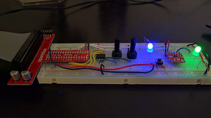
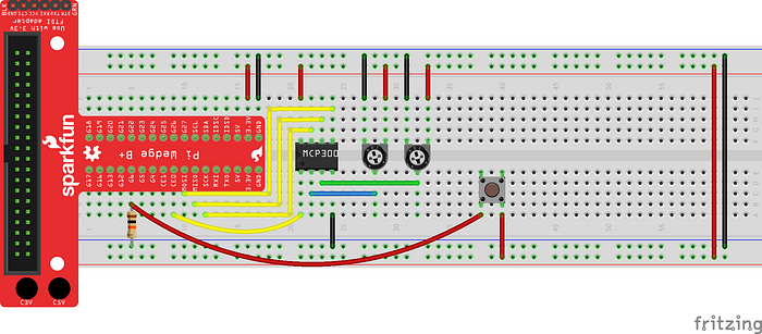
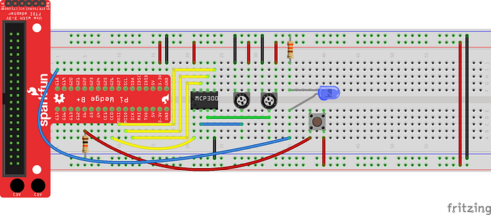
The Circuit
The scenario I’ll be working with is fairly straightforward: the Raspberry Pi will read in a voltage from a potentiometer and accordingly dim or brighten an LED. Of course, it’s not very practical as you can directly connect the potentiometer to the LED to achieve the same effect, but using the Raspberry Pi as the redundant middle-man requires both analog input and analog output and the premise is simple enough for a beginner.
I’ll actually be wiring up two potentiometers and outputting respectively to two LEDs to demonstrate the two-channel capabilities of the ADC I’ve chosen (MCP 3002) and to demonstrate Android Things built-in PWM functionality for “simulating” analog output vs. generating the real analog signal with a DAC (MCP 4725).
Finally, I decided to add in a pushbutton to start and stop reading from the potentiometers and outputting to the LEDs.
The final diagram looks something like (generated with Fritzing):

(I’m using Sparkfun’s MCP 4725 DAC in the physical photo, but could only find Adafruit’s DAC Fritzing diagram — the wiring is essentially the same, but mirrored).
Analog Input
First, let’s focus on just the inputs: the pushbutton, two potentiometers, and the MCP 3002 ADC.
Mini Pushbutton — Not Quite Analog Yet
The pushbutton is the easiest component to start with and if you’ve already done the simple Android Things sample project, you’re already done! We’re not working with analog signals yet, and I’ll assume you can hook one up, but I wanted to call out a few things that beginners might miss.
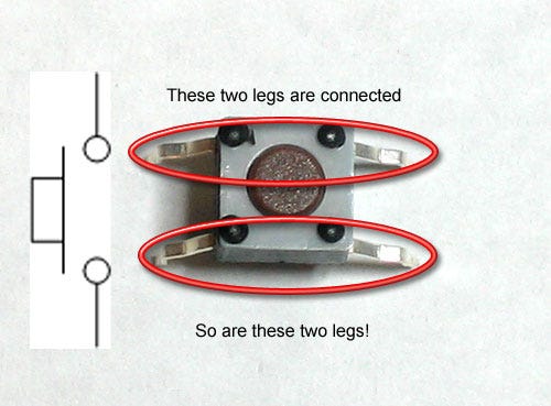
Make sure you have a pull-up or pull-down resistor on your input pin to ensure the line has a “default state” when the button is not pressed. I used a 10K Ohm pull-down resistor in my example, so the line is pulled LOW when the button is released or not being pressed. When pressed, the GPIO pin gets connected to the 3.3V source.
One caveat is the concept of debouncing. Basically, when you press or release a button, the HIGH or LOW signal may not instantly stabilize as you might expect. You have a chance that the signal may oscillate for a second before stabilizing, which would cause your button listener to get false callbacks.

A fairly easy way to debounce using software is a simple timer that checks that the signal has not changed (i.e. has stabilized) after a set period of time. If you’re using the sample Button driver from the contrib-drivers repo, it already has a built-in setDebounceDelay(long) method you can call that does just that! Though, you can just kick off your own delayed Runnable to check for the stable signal if you don’t want to pull in the driver.
enableBtn = new Button(ENABLE_BUTTON_PIN_NAME,
    Button.LogicState.PRESSED_WHEN_HIGH);
enableBtn.setDebounceDelay(BUTTON_DEBOUNCE_DELAY); // Ex. 50 ms
enableBtn.setOnButtonEventListener(...); // Start or stop the system
MCP 3002 ADC — Setup
Next, we need some way to read the voltage outputted by the two potentiometers.
I won’t belabor the process of wiring the pots up — usually one side gets GND, one side gets a positive voltage, like 3.3V (which side doesn’t matter, but it determines the direction in which the knob is twisted to affect the voltage), and the middle pin is the “output” somewhere in the range of 0–3.3V, dependent on the knob’s position.
We can’t connect the pot outputs to GPIO pins, as reading from them will only yield a (digital) HIGH or a LOW value — a 1 or a 0 — ON or OFF, so we need an ADC. I’ll be using the MCP 3002 ADC in this tutorial. It has two channels for sampling two different signals and is interfaced with using the SPI protocol (next section). It also has a 10-bit resolution, meaning the values used to represent the signal’s samples will range from 0–1023 unsigned to represent from 0V to 3.3V (the supply). If you need something with more channels, the MCP 3008 supports up to 8.
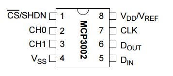
The datasheet has a diagram to let you know how to wire the chip up. Connect 3.3V to VDD and GND to VSS. One pot for each of the CHannel pins. The remaining four pins will all be used for SPI communication.
MCP 3002 ADC — SPI Communication Basics
The MCP 3002 is interfaced with using the SPI, or Serial-Peripheral Interface, communication protocol and support is baked into Android Things! In this context, “serial” refers to data being sent bit-by-bit vs. “parallel” where multiple bits are sent simultaneously.
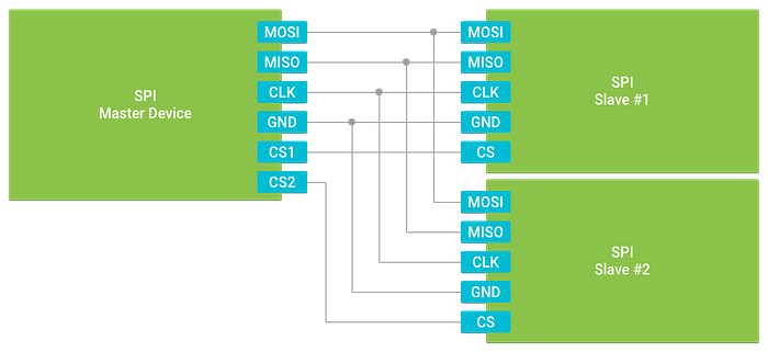
There are four pins required for SPI:
- MOSI — Master Out Slave In. The Raspberry Pi uses this line to send data to the ADC (slave).
- MISO — Master In Slave Out. The Raspberry Pi uses the line to read data from the ADC.
- CLK — A shared clock signal (driven by the Pi), so that data is transmitted on a synchronized interval.
- CS — A Chip Select pin used to enable the ADC. If we had multiple ADCs, we have multiple CS lines so that we could select which one to talk to.
Although it requires 3 dedicated pin + 1 CS pin for each slave device, SPI is relatively simple to understand and can support higher rates of data transfer, in comparison to I²C, which I’ll discuss in the Analog Output section.
The Raspberry Pi also has these exact pins, so they can be connected to the ADC now:
- MOSI gets connected to DIN (data in).
- MISO gets connected to DOUT (data out).
- CLK to CLK.
- CS0 to CS (we don’t need to use the Pi’s other Chip Select pin). If you have a breakout for the Pi’s pins, this might be called CE0 (Chip Enable) or SS0 (Slave Select).
Opening the SPI connection is pretty straightforward from the Android Things page.
SpiDevice adc;...// Pass in the name from PeripheralManagerService#getSpiBusList
public void connect(String spiName) throws IOException {
    PeripheralManagerService peripheralManagerService =
        new PeripheralManagerService();    adc = peripheralManagerService.openSpiDevice(spiName);
    ...
But things get a little interesting when it comes to setting up the initial configurations.
MCP 3002 ADC — SPI Configuration
First, we need to know what frequency the ADC expects the clock to be. Pages 2 and 3 of the datasheet list out the technical specs of the chip, which may seem intimidating if you’re a beginner, but we’re only interested in looking for one thing: the clock frequency, which appears on page 3 under the first entry for Timing Parameters:
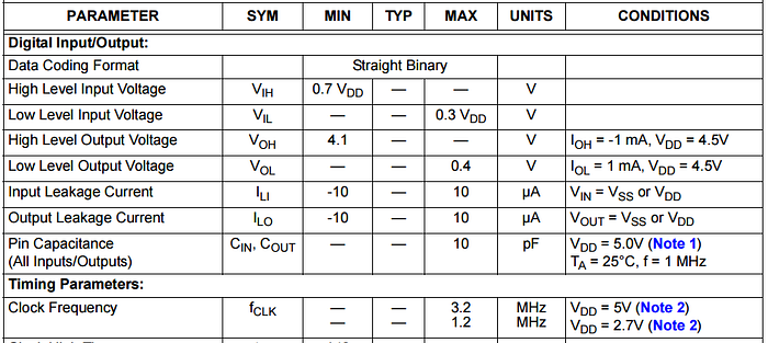
We’re told that the max frequency that is supported (or was tested) is 1.2 MHz when the supply voltage is 2.7V and is 3.2 MHz when the supply voltage is 5V. Meaning simply that more power means it can support a faster data rate. Since we’re powering the chip with 3.3V, we can be pretty confident that 1.2 MHz will work.
adc.setFrequency(1200000); // 1.2 MHzAlso related to the clock, we need to set the SPI Mode, which defines the idle state of the clock when data is not being transferred (LOW or HIGH) and whether bits get sampled when the clock goes low-to-high (rising edge) or high-to-low (falling edge) — once sampled, the next bit is transmitted on the following edge (ex. sample on the falling edge, transmit on the rising edge).
There are four permutations of these options and can be represented as a tuple of two binary numbers (X, Y) or taken together as a two-bit binary digit:
- Mode 0,0 (or Mode 0) — Low CLK idle, sample on the rising edge.
- Mode 0,1 (or Mode 1) — Low CLK idle, sample on the falling edge.
- Mode 1,0 (or Mode 2) — High CLK idle, sample on the rising edge.
- Mode 1,1 (or Mode 3)-High CLK idle, sample on the falling edge.
The Android Things docs use the word “transferred” instead of “sample” which I’m assuming is meant as an abstraction. Later I’ll show a screenshot of bits being sent overlaid with the clock pulses.
Now that the different mode “codes” are known, we can see on the first page of the datasheet that the ADC supports either Mode 0,0 or Mode 1,1.
adc.setMode(SpiDevice.MODE0);Finally, we can also set the number of bits per word (ex. number of bits transmitted in one shot — may not necessarily transmit 8-bits at a time) and also whether or not the data will be sent from Most Significant Bit (MSB) to Least Significant (LSB) or vice versa (remember the “S” in SPI stands for “Serial”, so both parties have to agree on what order they’re sent). Android Things has defaults for these, but it doesn’t hurt to explicitly call out.
The datasheet mentions transmitting digital readings as bytes (8 bits) and timing diagrams indicate the MSB should arrive first.
adc.setBitsPerWord(8);
adc.setBitJustification(false); // MSB first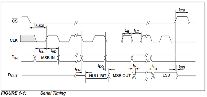
The final configuration for the ADC in code is then:
private SpiDevice adc;

public Mcp3002(String spiName) throws IOException {
    connect(spiName);
}

public void connect(String spiName) throws IOException {
    PeripheralManagerService peripheralManagerService = new
        PeripheralManagerService();
    adc = peripheralManagerService.openSpiDevice(spiName);
    adc.setMode(SpiDevice.MODE0); // CLK low, sample on rising edge
    adc.setFrequency(1200000); //  1.2 MHz
    adc.setBitsPerWord(8);
    adc.setBitJustification(false); // MSB first
}
I wrapped the ADC interactions in a wrapper object, following the contrib-drivers repo format.
MCP 3002 ADC — Reading Data
Now we have the connection to the ADC established and configured, we can finally start asking it for converted digital values for the two potentiometers!
Communications with the chip are defined on pages 15 and 16 of the datasheet. To get one reading, all we need to do is transmit a few command / configuration bits to it after the clock and the chip select trigger together to indicate the start of communications:
- A start bit (HIGH)
- A bit to signify two-channel mode (HIGH)
- A bit to indicate which channel (CH0 or CH1) to read from (LOW or HIGH)
- A bit to indicate whether we want the reading sent back MSB first or LSB first (LSB first mode transmits first in MSB first mode, then concatenates the LSB representation). We can just use MSB mode, so HIGH.
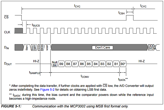
We can’t stop transmitting there, though. According to the datasheet, the ADC will transmit the readings back almost immediately after the MSBF bit is transferred (following one clock cycle and a null bit). If we stop transmitting, the Chip Select (CS) line will go back high and per the datasheet:
If it is desired, the CS can be raised to end the conversion period at any time during the transmission.
We know the chip is a 10-bit ADC. So we need to send at least 11 more bits (room for the null bit + 10 bits of data) to keep the CS open for the data to come back to us over the MISO line. These 11 bits can be anything (signified as “Don’t Care” in the diagram above). After the 11 bits, if we were to continue transmitting, it would not cause any problems:
any further clocks with CS low, will cause the device to output zeros
So, the total amount of bits we need to send to get one 10-bit analog-converted-to-digital reading from the ADC:
- 4 command / configuration bits
- 11 don’t cares
15 bits. We can pad on one 0 at the beginning to make it an even 2 bytes. This is also called out as supported in the datasheet :)
If necessary, it is possible to bring CS low and clock in leading zeros on the DIN line before the start bit. This is often done when dealing with microcontroller-based SPI ports that must send 8 bits at a time.
So, we’ll be sending:
011C 1XXX XXXX XXXX (where C = channel (0 or 1) and X’s = don’t care)
We can use 0’s for the don’t care:
011C 1000 0000 0000
Leaving us with two hex values to represent the data, depending on the channel:
- Send 0x68 0x00 to read from channel 0
- Send 0x78 0x00 to read from channel 1
Can you both read and write over SPI at the same time (full-duplex) on Android Things? Yep! Just use SpiDevice#transfer(txBuffer, rxBuffer, txLength).
Here’s what the code looks like. Instead of defining two different datasets to write depending on the channel, I just shift the 0 or 1 into the right spot.
/**
 * Data transfer for reading is explained on page 15 of the datasheet.
 * - First five control bits are (for two-channel mode):
 *     - A 0 bit for padding
 *     - Start bit (1)
 *     - Two-channel mode indicator (1)
 *     - Channel select (0 = channel 0, 1 = channel 1)
 *     - MSBF vs. LSBF (0 = LSBF, 1 = MSBF)
 * -   Then, 11-bits of Don't Cares are transmitted while the slave
 *     responds with the null bit + 10-bit analog value at the same
 *     time.
 */
public int analogRead(AdcChannel channel) throws IOException {
    byte[] txAdc = new byte[2];
    byte[] rxAdc = new byte[2];    // Prepare the command to send to the ADC
    txAdc[0] = (byte) (0x68 | channel.ordinal() << 4);
    txAdc[1] = (byte) 0x00;    // Write & read simultaneously
    adc.transfer(txAdc, rxAdc, rxAdc.length);    // Print readings
    Timber.d("R/W ADC MCP 3002: channel %s, tx %s, rx %s",
        channel.ordinal() + 1, Arrays.toString(txAdc),
        Arrays.toString(rxAdc));    // Merge the two bytes read into one int
    return (rxAdc[0] & 0x03) << 8 | (rxAdc[1] & 0xFF);
}
...
public enum AdcChannel {
    CHANNEL_0,
    CHANNEL_1
}
Once we get the reading back, remember that it’s split across two bytes like this:
000000XX XXXXXXXX
You’ll need to shift the two least-significant bits in the first byte over to positions 8–9 before ORing it with the second byte. Ex:
  000000XX00000000
| 00000000XXXXXXXX
------------------
  000000XXXXXXXXXX
If all goes well, you can start getting some 10-bit numbers by calling this method in a loop (triggered by the mini pushbutton)!

If you want to convert them to the approximated voltage (between 0 and 3.3V), you can use a ratio:
int pot1Reading= analogRead(CHANNEL_0);
double pot1Voltage = ((double)reading / 1023) * 3.3;
With the readings in the above log screenshot:
- Channel 0— [0, 39] => 39 (Base 10) ~= 0.126V
- Channel 1— [2, -59] => 709 (Base 10) ~= 2.2V
MCP 3002 ADC — Viewing SPI on the Oscilloscope
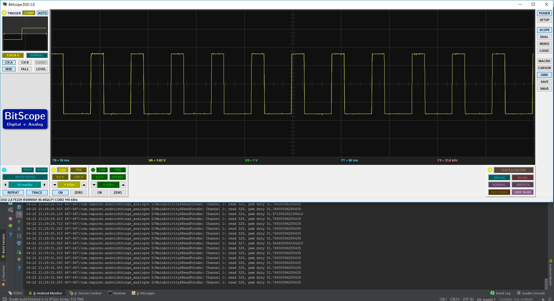
Since I got my hands a nice, cheap oscilloscope, I thought it’d be interesting to see the communication on the wire to see if it’s really happening the way you expect it to.
Let’s just focus on reading Channel 0. First, we expect 0x68 0x00 to be transmitted. Below is what the scope captures. The yellow line is monitoring MOSI and the green line is monitoring the CLK. Note, both signals peak at 3.3V, but I’ve independently halved the scale of the CLK signal, so that it is easier to view the data on MOSI.

Remember that we’re using SPI Mode 0,0, which means the clock idles low, data is sampled on the rising edge, and data is transmitted on the falling edge. If we take a look at what the signal looks like at each rise of the clock, we can make out 01101000 00000000 = 0x68 0x00. Nice!
Here’s what the response looks like. The yellow signal is now monitoring MISO.

In this case, logcat was printing rx [2, 10] , which is 0x02 0x0A = 522 (base 10) = approx. 1.68V.
Remember, during the first 5 clock cycles of the “received” signal above, we’re actually doing the transmission of 0x68 0x00 shown two screenshots ago. So, if we look at both the MOSI (yellow) and MISO (green) signals together…

My oscilloscope only has two channels, so I can’t show you the clock, but here we see the first 5 transmitted bits followed immediately after by the null bit, then the 10-bits sample of the analog signal.
Viewing the communication on a scope can really help you understand (and also debug) what’s actually happening behind the scenes, if you can shell out a little cash for one. In this case, we are able to visually verify that the SPI communication happens exactly like we expect it to.
Analog Input — Conclusion
Although you have to wire up an external chip, read a datasheet, and use SPI communication, analog reading functionality can really expand the space of what you can do in your IoT projects. Understanding SPI also enables you to work with much more than a simple ADC chip.
Analog Output
At this point we have a push button set to start / stop the system and we are able to read from our two potentiometers through our MCP 3002 ADC. Next, the goal is to take these 10-bit readings (representing some voltage between GND to 3.3V) and output them back out to some LEDs.
The only problem: the Raspberry Pi can’t output from its GPIOs anything except GND or 3.3V— it can’t perform analog output in the way we expect.
We have two options, we can use Pulse-Width Modulation (PWM) to “simulate” a desired voltage, which is already built into the Raspberry Pi and Android Things, or we can use an external digital-to-analog converter (DAC).
Lighting an LED — Pulse-Width Modulation
If we can only output GND or 3.3V, what would happen if we hooked up to an LED and toggled between these two states very quickly — sort of like a clock signal? This is the basic idea of Pulse-Width Modulation (PWM) and the idea is that, by varying to lengths of when the signal is LOW vs. HIGH, the signal’s perceived voltage approaches the average of the LOW/HIGH periods.

The duty cycle defines the percentage of each cycle that the signal is kept HIGH. It’s fairly straightforward to calculate the voltage of a PWM signal — take your HIGH level (in our case 3.3V) and multiply it by the duty cycle. So, a 50% duty cycle will yield 1.65V, a 10% duty cycle will yield 0.33V, etc.
Android Things supports PWM and you only need to worry about the signal’s frequency and duty cycle. The frequency will depend on your use-case. We want to use PWM to dim an LED without being able to visually notice the PWM switching, so 120 Hz is an adequate frequency here. It’s a lower frequency, but high enough that your eyes won’t be able to discern the switching.
I decided to create a PwmLed class to wrap the LED we’ll be lighting with PWM.
private Pwm led;
...public void connect(String pwmName) throws IOException {
    PeripheralManagerService peripheralManagerService = new
        PeripheralManagerService();
    led = peripheralManagerService.openPwm(pwmName);
    led.setPwmFrequencyHz(DEFAULT_FREQUENCY);
}public void setDuty(double duty) throws IOException {
    led.setPwmDutyCycle(duty);
    led.setEnabled(true);
}
Next, we want to light the first LED using PWM, based on the readings we get from the first potentiometer.
Remember, our ADC returns a 10-bit number to digitally represent an analog signal, so we have to convert it to the corresponding duty cycle between 0 and 100. For example, a reading of 512 from the ADC corresponds approximately to 1.65V, which we could output using a PWM signal at 50% duty.
private void readAndSetLedWithPwm() throws Exception {
    int reading = adc.analogRead(AdcChannel.CHANNEL_0);

    // Convert reading to a percentage for the duty cycle
    double duty = ((double) reading / 1023) * 100;

    Timber.d("Channel 1: read %s, pwm duty %s", reading, duty);
    pwmLed.setDuty(duty);
}
If we check out the PWM signal on the oscilloscope, we can see the duty cycle change as the potentiometer is adjusted.

Lighting an LED — Using the MCP 4725 DAC
We can also use a DAC to generate the actual voltage we’re looking for, rather than approximating it using PWM. The Raspberry Pi does not have a built-in DAC, so we have to hook up an external chip, like we did with the ADC. I’ll be using the MCP 4725. It uses I²C for communication, so we get to try that out with Android Things and it also has a small amount of EEPROM, so you can have it “remember” what to output when it’s initially powered on. Finally, it’s also a 12-bit DAC, meaning it has 4096 steps of analog voltages it can output between GND to 3.3V (its supply). Pretty precise!
After this, we’ll also have the complete circuit finished.
MCP 4725 — I²C Communication Basics
Inter-Integrated Circuit (I²C) is another serial communication bus with support in Android Things, like SPI. Like SPI, the communicating parties synchronize by sharing a clock — the serial clock (SCL). However, I²C gets away with only one other line — a shared serial data line (SDA).
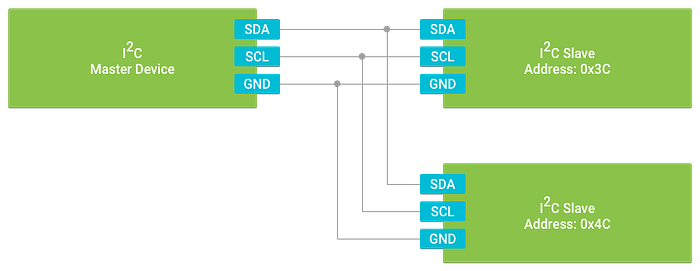
In SPI, the master indicates which slave to talk to by explicitly enabling that slave using one of the Chip Select lines. In I²C, listeners on the bus have set addresses (typically hardcoded into the device). The master emits the address of who it intends to talk with onto SDA before communications happen. This is great because it scales very well, you only need two pins for I²C, regardless of how many devices you want on the bus.
Some tradeoffs compared to SPI are: (1) the transmission of the slave address is pure overhead; (2) you can’t send and receive data at the same time (half-duplex).
I²C communciation is a little more complex — with rules defining how multiple masters can operate on the same bus and how a slave device can acknowledge data reception or slow down the master if its transmitting too quickly — but the basic communication model is:
- The master device transmits the address of the slave device it wishes to talk to on the SDA line.
- The master writes data on the SDA line or awaits the slave to send data back. Other devices on the line can ignore the data if it’s address was not previously specified.
There is also a concept of “registers” or “commands” that the master device can read from or write to and are usually specified with addresses as well. For example, reading data from an accelerometer via I²C might look like:
- Master transmits the accelerometer’s I²C address on SDA for reading.
- Master transmits the address of the accelerometer’s X-coordinate register on SDA.
- Accelerometer responds with the X-coordinate data on SDA.
- SDA and SCL allowed to return to an idle state.
Wiring the chip up is pretty simple. Both the Sparkfun and Adafruit breakouts have pins for GND, VCC (3.3V), SDA, and SCL.
MCP 4725 DAC — I2C Configuration
To communicate with the MCP 4725 over I²C, we’ll need to look at the datasheet to find out:
- The I²C address.
- The command / register to indicate to the DAC — we want to let it know we are sending data to be outputted as an analog signal.
- How we send said data to the DAC.
That’s about it. Unlike SPI, we don’t have to specify a “mode” for the clock & sampling time, as its already specified in the standard (clock idles low, sampling is done on the rising edge). We also don’t have to worry about setting an explicit frequency.
Page 23 of the datasheet covers the I²C operation of the DAC. I²C addresses are actually 7-bits (though, there is a way to do 10-bits). The datasheet states:
The MCP4725 device address contains four fixed bits ( 1100 = device code) and three address bits (A2, A1, A0). The A2 and A1 bits are hard-wired during manufacturing, and A0 bit is determined by the logic state of A0 pin.
…
The A2 and A1 are programmed to ‘00’ (default), if not requested by customer. A0 bit is determined by the logic state of A0 pin.
So far, we have 110 000X, where X = A0
The Sparkfun and Adafruit offerings of the MCP 4725 allow you to wire A0 to GND or your voltage supply to create two different addresses: 110 0000 and 110 0001. This means you could have two MCP 4725s in your circuit and address them independently (otherwise, you’d have problems because they’d both respond to the same I²C address). In our case, we’re not going to mess with A0, so it’ll just be grounded. This gives us the final address of: 110 0000 or 0x60. You can now open the I²C port on Android Things (again, I’m wrapping this into a method call in a Mcp4725 class):
// I2C bus name is "I2C1" on my board. Address is 0x60.
public void connect(String i2cName, int i2cAddr) throws IOException {
    PeripheralManagerService peripheralManagerService = new
        PeripheralManagerService();
    dac = peripheralManagerService.openI2cDevice(i2cName, i2cAddr);
}
MCP 4725 DAC —Writing to the DAC
Page 23 of the datasheet also defines the different commands for writing to the DAC, with communication diagrams given on the subsequent pages.
Basically, we have the choice of: (1) writing to the DAC’s register for outputting as an analog signal; or (2) performing (1) and also writing the value to EEPROM so that it is remembered the next time the circuit is wired up. We also know this is a 12-bit DAC, so we have to specify both the write command and then send 12-bits of data.
Note: there is also a “Fast” write mode we can use (which does not need a command — all you do is send your 12-bits of data), but I’d like to show how to use one of the actual commands.
Since writing to the EEPROM will take a little extra time, we can do without it and just stick with writing to the DAC register. Here’s the communication diagram we can reference:
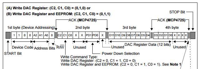
Looks like we need four bytes:
- The address byte. Android Things takes care of this one for us when we use it to read or write to an I²C device. It’s only the 7-bit address and one extra bit for specifying a read or a write. This is pretty standard.
- The command byte. We need to specify the bits to indicate the command (C2, C1, C0) and two power control bits (PD1, PD0). Some unused bits too.
- Two bytes for our 12-bits of data (last four bits unused).
We already know our 3 command bits from the datasheet. Writing to the DAC register w/o EEPROM = 0 1 0. The power control bytes are on page 20, but the default is 0 0. We’ll use 0’s for the unused, so our command byte looks like: 0100 0000 or 0x40.
For the 12-bits of data, we’ll just make sure we do some shifting to get our data in the right format. No big deal.
We can just prepare a byte buffer and use the basic write method to do this:
    // Writes to our DAC which will do analog output on our behalf
    public void analogWrite(int val) throws Exception {
        byte[] writeCmd = new byte[3];
        writeCmd[0] = WRITE_MODE | POWER_DOWN_DEFAULT_MODE; // 0x40
        writeCmd[1] = (byte) (val >> 4);
        writeCmd[2] = (byte) (val << 4);

        Timber.d("Writing to DAC MCP 4725: %s",
            Arrays.toString(writeCmd));
        dac.write(writeCmd, writeCmd.length);
    }
And that’s it! We can start sending 12-bit values to our DAC. To connect this up with the ADC readings from our second pot, we just need to make sure we convert the ADC’s 10-bit readings into the appropriate range for our DAC (12-bit).
private void readAndSetLedWithAnalog() throws Exception {
    int reading = adc.analogRead(AdcChannel.CHANNEL_1);

    // Convert from ADC's range to the DAC's range
    reading = (int) (((double) reading / 1023) * 4095);

    Timber.d("Channel 2: read %s, sending to DAC", reading);
    dac.analogWrite(reading);
}
MCP 4725 DAC— Viewing I²C on the Oscilloscope
There’s 4 bytes being transmitted every time we want to update the DAC, so getting it all to fit on screen might look a little squished. In general, we should expect to see:
- The DAC’s I²C address — 0x60.
- The write command — 0x40.
- 12-bits of data.
In this next screenshot, the Pi is sending the value 2898 to the DAC. The SDA is in yellow and the SCL is in green. Like the SPI screenshots, I cut the scale of the clock in half for easier visibility.

In I²C, acknowledgement (ACK) bits follow every byte, which I’ve colored grey. They also help visually break the transmissions into the individual 8-bit bytes. So, we have:
- Addr = 1100 0000 = 0xC0. Hmm, that doesn’t seem right, we were expecting the 0x60. However, remember that the I²C addresses are 7-bits, after which they are followed by a R/W bit (W= 0). So, the full byte is 1100 0000 = 0xC0.
- Cmd = 0100 0000 = 0x40.
- Data = 1011 0101 0010 (followed by the 4 unused bits) = 0x0B52 = 2898 (Base 10).
MCP 4725 DAC — Compared to PWM
We can also use the oscilloscope to view the same voltage being generated by both the DAC and PWM. Here, the pots have been adjusted so that both generate 1V (yellow = PWM, green = DAC output):

Analog Output — Conclusion
If you need analog output in your Android Things circuits, you have two options. You can use the built-in PWM functions to approximate the voltage you want using averages. You can also hook up an external DAC to get the actual analog signal you want. I²C is a pretty versatile communication protocol to understand as well and is used in as many places (maybe more) as SPI.
Closing
The ultimate goal of this tutorial was to show you how to do Analog I/O with the Raspberry Pi. Besides the built-in PWM function for analog output, we had to resort to using external chips for general purpose analog I/O. The MCP 3002 ADC and the MCP 4725 DAC were used, which required an understanding of SPI and I²C, respectively. Working with hardware often means you have to look through the datasheet to get what you know — this can often seem intimidating, but can be mitigated if you keep in mind what exactly you’re looking for. Finally, I provided screenshots of these various signals from an oscilloscope, which can help you verify that the system operates as you expect it to.
The full code for this tutorial, including the Arduino sketch in the next bonus seciton, can be found on my GitHub:
https://github.com/NickCapurso/AndroidThings-RaspPi-AnalogReadWrite
Bonus — Proxying through an Arduino to the DAC
Initially I tested out the MCP 4725 on my Arduino, since there are already existing tutorials for using it with the Arduino. For fun, I wanted to try sending the data from my Raspberry Pi to the Arduino for it to forward on to the DAC. This also demonstrates a scenario where there are 3 devices on the I²C bus, one of which (the Arduino) acts as both a master (to the DAC) and a slave (to the Pi).
The code from the Raspberry Pi is exactly the same as before, except the I²C address is different (I arbitrarily chose 0x77) and we don’t need to send the 0x40 command byte, as the Arduino will do that for us:
public void analogWrite(int val) throws Exception {
    byte[] writeCmd = new byte[2];
    writeCmd[0] = (byte) (val >> 4);
    writeCmd[1] = (byte) (val << 4);    Timber.d("Writing to DAC thru Arduino: %s",
        Arrays.toString(writeCmd));
    dac.write(writeCmd, writeCmd.length);
}
The code on the Arduino side is as you might expect. The Wire library is used for I²C and you can setup a callback function when data is received on SDA. Using the library, you can pick any address you want for the Arduino to respond to.
#include <Wire.h>#define I2C_ADDR 0x77
#define MCP4725_ADDR 0x60
#define MCP4725_WRITE_MODE 0x40
#define POWERDOWN_DEFAULT_MODE 0x00// 12-bit value == top8 bits + bottom 4 bits (pre shifted) (+ 4 don't cares)
byte top8;
byte bottom4;void setup()
{
  top8 = 0;
  bottom4 = 0;

  Wire.begin(I2C_ADDR);
  Wire.onReceive(onI2CReceived);
}void onI2CReceived(int numBytes) {
  if (Wire.available() >= 2) {
     top8 = Wire.read();
     bottom4 = Wire.read();
     while(Wire.available()) {
      Wire.read();
     }
  }
}void loop(){
     delay(250);
     Wire.beginTransmission(MCP4725_ADDR);
     Wire.write(MCP4725_WRITE_MODE | POWERDOWN_DEFAULT_MODE);
     Wire.write(top8);
     Wire.write(bottom4);
     Wire.endTransmission();
}
I had issues writing to the MCP 4725 during onI2CReceived . I’m guessing it’s because you’re still currently receiving on SDA and you can’t immediately write out at the same time, as I²C is half-duplex. So, instead, the DAC gets updated during loop.